The U.S. semiconductor industry is undergoing a massive transformation, driven by the CHIPS Act of 2022. With over 140 projects announced since 2020, totaling $645.3 billion in private investments, the construction of semiconductor fabs is reshaping the nation's manufacturing landscape. Key highlights include:
The CHIPS Act has catalyzed a surge in demand for mission-critical construction management expertise, with companies racing to recruit skilled professionals for these highly complex projects. Meeting workforce demands and adhering to regulatory requirements are critical for ensuring these fabs are completed on time and within budget.

U.S. Semiconductor Fab Construction: CHIPS Act by the Numbers (2026)
As of May 2026, the U.S. is witnessing a semiconductor construction boom, with $85 billion worth of projects actively underway and an additional $632 billion or more in planning and engineering stages [6][3]. This surge is reshaping where construction management (CM) expertise is most in demand, creating an urgent need for skilled professionals to tackle these ambitious builds. The following breakdown highlights the key states and regions driving this transformation.
Arizona and Ohio are leading the charge, each hosting approximately $28 billion in active projects [6]. Arizona is home to TSMC's Fab 21 campus in Phoenix, where the company has committed $165 billion across four planned fabs. Notably, the second fab began pilot production in early 2026, six months ahead of schedule, with full-scale production expected by Q1 2027 [1][6]. Meanwhile, Ohio anchors Intel's massive Project Cardinal and Project Dragonfly in New Albany, bolstered by a CHIPS Act award finalized in November 2024 [13].
Idaho ranks third, driven by Micron Technology's $25 billion fab expansion in Boise [6]. Looking ahead, New York is poised to take the lead in future construction, with Micron breaking ground in January 2026 on a $100 billion megafab in Clay - the largest private investment in the state's history. The first phase is targeted for completion by 2030 [7][1]. Texas also remains a key player, with Samsung's $17 billion Taylor facility aiming to be operational by 2026 after resuming full-scale construction in mid-2025 [7][1].
These investments highlight how demand for CM expertise is spreading beyond traditional industrial hubs. Projects in states like New York and Ohio underscore the need for specialized talent to manage the unique challenges of semiconductor construction.
| State | Key Companies | Investment Scale | Status (May 2026) |
|---|---|---|---|
| Arizona | TSMC, Intel, Amkor | ~$28B (Active) | Fab 21 Phase 2 in pilot production |
| Ohio | Intel | ~$28B (Active) | Final CHIPS award granted Nov 2024 |
| Idaho | Micron | ~$25B (Active) | Fab 4 expansion underway in Boise |
| New York | Micron, GlobalFoundries | $100B+ (Planned) | Clay megafab broke ground Jan 2026 |
| Texas | Samsung, TI, GlobalWafers | $37B+ (Active) | Taylor fab targeting 2026 operations |
| Utah | Texas Instruments | ~$11B (Active) | Lehi 300mm fab targeting 2026 production |
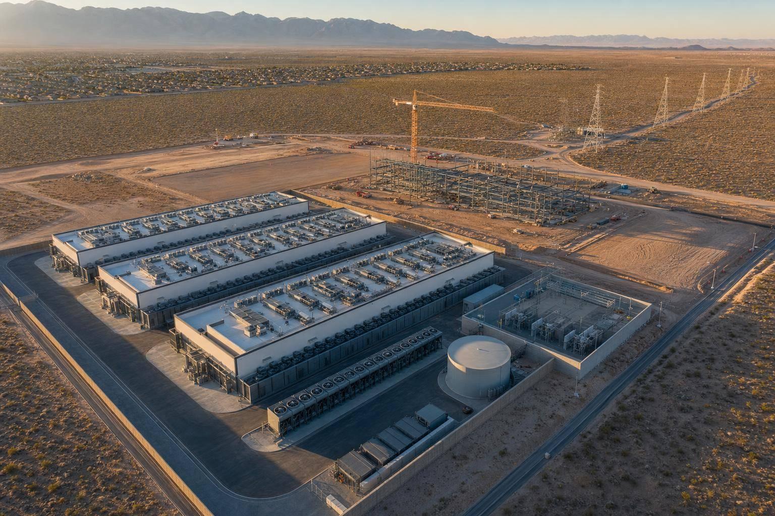
Building semiconductor fabs is a whole different ballgame compared to other industrial projects. These facilities demand cleanrooms exceeding one million square feet, ultra-pure water systems, and specialized gas and HVAC systems capable of supporting sub-five-nanometer chip production [10][1]. Adding to the complexity, Extreme Ultraviolet (EUV) lithography equipment requires installation with near-zero vibration, influencing everything from foundation design to construction sequencing [1].
Permitting and regulatory hurdles further complicate these projects. U.S. fabs often face longer preconstruction timelines compared to international counterparts due to federal environmental reviews and multi-agency approvals [9]. For instance, Micron's Clay megafab experienced a two-year delay in its groundbreaking schedule due to environmental reviews and construction complexities [11][1]. Additionally, CHIPS Act compliance introduces new obligations, such as adhering to Davis-Bacon Act wage rules, detailed cost reporting, and a 10-year restriction on expanding manufacturing in certain countries [2].
"The United States currently builds fewer fabs at a slower rate than the rest of the world. Part of the reason for this is permitting regulations which require long assessment timelines." - John VerWey, Center for Security and Emerging Technology [9]
These technical and regulatory demands are reshaping workforce needs, pushing the industry to adapt quickly to meet the unique challenges of fab construction.
The CHIPS Act is expected to generate 122,000 construction jobs across the 52 funded projects [3][13]. A single large-scale fab can require 10,000 to 15,000 workers during peak construction phases [12]. For example, Samsung's Taylor campus supported 8,868 direct and 9,768 indirect construction jobs in 2024 [1]. Micron's U.S. expansion, covering Idaho, New York, and Virginia, is projected to create 90,000 direct and indirect jobs over time [7][1].
However, many of these projects are being built in areas with limited semiconductor labor pools. New Albany, Ohio, and Clay, New York, are emerging as major hubs despite a lack of local expertise in this specialized field [8][1]. Leading engineering firms are responding by scaling up aggressively. Jacobs, for instance, reported a 12.3% revenue increase in early 2026, driven by semiconductor and data center projects. Similarly, Fluor has hired senior executives from Bechtel to spearhead its Advanced Technologies unit [14].
"The workforce cannot be created on the timeline that fab construction permits." - Amtec Staffing [8]
This mismatch between construction timelines and workforce availability is the central challenge for CM leaders today, as more projects transition from planning to active construction.
The challenge in semiconductor fab construction isn't just about filling positions - it's about finding the right expertise. Building these facilities requires a skill set far beyond what's needed for typical industrial projects. Bridging the gap in both technical know-how and leadership capabilities is key to addressing the workforce shortage discussed earlier. Identifying the critical roles and their importance is the foundation for assembling a team capable of tackling these complex projects.
Leadership in fab construction is multifaceted and extends well beyond basic project timelines. For example, a Preconstruction Manager must handle logistics like oversized load routing, bridge certifications, and freight coordination for highly sensitive equipment such as ASML's EUV systems. These machines are so critical that a single mishap during transport could delay production by an entire year[12].
Compliance Managers are equally vital, especially for projects funded under the CHIPS Act. They oversee Davis-Bacon Act wage audits, apprenticeship reporting, and "Buy America" compliance - requirements rarely encountered in private industrial builds[5]. Companies lacking a dedicated compliance framework may find it difficult to compete for these projects. For additional insights into workforce planning on large-scale construction projects, check out iRecruit.co's guide to jobs and workforce in construction.
While leadership roles set the tone, technical specialists ensure the intricate systems in fabs operate flawlessly.
Fab construction demands technical expertise that goes far beyond conventional industrial standards. Take Process Piping Specialists, for instance - they manage ultra-high-purity gas and chemical systems that require purity levels of 99.9999%, measured in parts per trillion[12]. Standard plumbing experience doesn't cut it here.
"Something that passes code in a conventional industrial facility will completely fail in an ultra-clean PCMP environment." - Kaushik Krishnan, Licensed Professional Engineer[4]
Commissioning Managers focus on certifying critical systems like ultra-pure water, specialized HVAC, and cleanroom environments[1]. Meanwhile, MEP Project Managers ensure that mechanical, electrical, and plumbing systems function as a cohesive unit. Another key role is that of EUV Installation Specialists, who manage the setup of lithography machines valued at $350 million or more. These installations require precision down to near-zero vibration tolerances, influencing foundation designs from the start[1][12].
| Role | Core Responsibility |
|---|---|
| Preconstruction Manager | Oversized load routing, equipment logistics, bridge certifications |
| Compliance Manager | Davis-Bacon Act wage audits, apprenticeship goals, domestic sourcing |
| Process Piping Specialist | Ultra-high-purity gas and chemical distribution systems |
| Commissioning Manager | Ultra-pure water systems, cleanroom certification, HVAC validation |
| MEP Project Manager | Integrated mechanical, electrical, and plumbing coordination |
| EUV Installation Specialist | Lithography machine installation and seismic isolation oversight |
Technical expertise is just one part of the equation. Successful fab construction also hinges on strong soft skills. Leaders in this field must blend engineering precision with the ability to manage large-scale human logistics. With peak construction sites requiring up to 15,000 workers[12], coordinating housing, transportation, and workforce morale becomes an operational necessity.
"The companies that scale best are the ones that combine urgency with discipline. They move quickly, but they do so through strong engineering systems rather than around them." - Kaushik Krishnan, Licensed Professional Engineer and Global Manufacturing Leader[4]
Another critical leadership trait is risk-based decision making. In March 2026, a global manufacturing team led by Kaushik Krishnan avoided $200 million in potential rework and downtime costs by accelerating time-to-market by four months. This was achieved through rigorous qualification of mechanical components across more than 20 suppliers and 200 hardware parts[4]. Such outcomes underscore the importance of treating every design approval as a key risk assessment step.
Hiring for semiconductor fab construction isn't just about identifying the right roles - it's about knowing when to hire and where to find the right talent. The process is particularly challenging given the specialized expertise required for these projects and the fierce competition for skilled professionals.
Semiconductor fab projects unfold in distinct phases, each requiring unique expertise. Take Micron's $100 billion megafab in Clay, New York, for example. Construction began in January 2026, with production slated for 2030. Early stages rely heavily on civil and structural specialists, while later phases demand expertise in MEP (mechanical, electrical, and plumbing) coordination, ultra-high-purity systems, and commissioning [1].
To avoid delays, it's critical to start recruiting specialized mechanical and electrical construction managers (CMs) at least a year before the tool-in phase. This is especially important for CHIPS Act-funded projects, where federal funding is tied to milestone completion [3]. Missing these milestones can delay reimbursements, creating financial and scheduling headaches.
TSMC’s Arizona expansion offers another example of phased hiring on a massive scale. By May 2026, the company was juggling multiple project phases simultaneously, each requiring different CM skill sets. This kind of parallel execution highlights the importance of planning workforce needs well in advance [1].
"Workforce availability is no longer a downstream consideration. It is a primary factor in whether projects stay on schedule, maintain quality, and achieve operational readiness." - iRecruit.co [15]
This phased approach to workforce planning is essential for securing the specialized talent needed for semiconductor fab projects.
The pool of fab-ready CM professionals is small and highly concentrated in regional hubs like Phoenix, the Dallas–Austin corridor, upstate New York, Boise, and Salt Lake City. With multiple large-scale projects competing for the same talent, staffing challenges on large-scale construction projects often mean traditional job postings fall short [1].
A more effective strategy involves targeting professionals from adjacent industries like data centers, energy infrastructure, and advanced pharmaceutical manufacturing. These sectors share the complexity, contamination-control protocols, and sequencing discipline required for fab construction. As iRecruit.co explains, "experience in mission-critical environments is often more important than general project scale" [15]. For more on how these skills translate, iRecruit.co’s guide on construction project delivery offers useful insights.
To address talent shortages, many project teams are adopting flexible staffing models. Blended approaches - combining permanent hires with project-specific contractors - can help overcome bandwidth issues, particularly during high-demand phases like the transition from construction to commissioning [15].
iRecruit.co specializes in recruiting for mission-critical sectors, including semiconductor fabs, data centers, advanced manufacturing, and energy infrastructure. Their services include executive search, embedded recruiting, and ATS implementation, all tailored to high-tech industrial projects [15].
For CHIPS Act-funded projects, iRecruit.co’s embedded recruiter model is especially effective. These embedded recruiters integrate into the project’s hiring framework, building scalable talent pipelines and pre-qualifying candidates for roles like Commissioning Manager, MEP Project Manager, and EUV Installation Specialist. Every candidate is vetted for the technical and regulatory expertise required in fab environments. To minimize risks of mis-hires, iRecruit.co also offers a 90-day search credit for replacements, ensuring projects stay on track and within budget.
The challenges outlined earlier - whether it's technical precision or workforce shortages - highlight the far-reaching effects of the CHIPS Act on construction management (CM) demand. With over $450 billion in private investments pledged toward domestic semiconductor manufacturing [16], the Act has reshaped the U.S. construction landscape, sparking an unprecedented need for specialized CM expertise.
To meet this demand, companies are ramping up efforts. Fluor brought on experienced leaders like former Bechtel executives John Palmer and Denis Bacon to spearhead its semiconductor construction initiatives [14]. Similarly, Jacobs saw a 25% year-over-year growth in advanced manufacturing projects by early 2026, resulting in a project backlog extending 12–18 months [14]. These trends point to a sustained shift in industrial construction, with ripple effects likely to extend well into the 2030s.
"The semiconductor construction pipeline represents a multi-decade commitment to domestic manufacturing capacity... it signals sustained demand for industrial construction expertise." - Westside Construction Group [1]
However, the workforce remains a critical bottleneck. By 2030, the U.S. is expected to face a shortage of 67,000 skilled workers, accounting for 58% of the new jobs created through CHIPS Act investments [16]. Addressing this gap will require deliberate and immediate action.
With demand reshaped, construction leaders must rethink their hiring strategies. Workforce planning now demands the same level of urgency as equipment procurement. As 360XStaffing emphasizes, "The talent you need for a TSMC facility, Phoenix build, is not sitting on Indeed waiting for your posting. They're already working - and contractors often begin recruitment 90 days before their needs peak" [17].
Filling key roles such as MEP superintendent, high-purity pipefitter, and VDC/BIM manager remains particularly challenging [17]. To bridge this gap, companies should consider:
For more insights, iRecruit.co’s guide on jobs and workforce in construction offers valuable strategies for aligning workforce planning with project outcomes.
At this pivotal moment, hiring decisions carry long-term consequences. By acting swiftly and strategically, construction leaders can ensure their teams are equipped to meet project demands and deliver on schedule.
The first hires for a CHIPS Act fab project should include project managers, construction managers, and engineering specialists. These roles are crucial for handling the design, planning, and execution stages. They ensure smooth coordination across the massive construction effort and maintain high standards throughout the project's lifecycle.
The CHIPS Act compliance rules introduce strict labor practices, safety standards, and timeline requirements that directly affect the construction schedules and staffing of semiconductor fabs. These regulations can lead to longer project timelines if not carefully managed. Additionally, they mandate a workforce trained in federal labor and safety protocols, which adds complexity to recruitment and workforce planning.
To navigate these challenges, proactive management becomes crucial. It helps ensure deadlines are met, compliance is maintained, and the growing demand for fab construction projects is addressed efficiently.
Industries such as advanced manufacturing, nuclear power, data centers, and large-scale industrial projects are excellent sources for fab-ready construction management talent. These fields demand specialized expertise, including precision construction, pipefitting, welding, and metal fabrication - skills that directly align with the needs of semiconductor fab plant construction.