Building a semiconductor fab is one of the most complex and expensive construction projects in the world. Costs range from $10 billion to $25 billion+, and timelines stretch 3 to 5 years from groundbreaking to first production. Delays and cost overruns are common due to challenges like long-lead equipment, supply chain constraints, permitting hurdles, and labor shortages. Missteps can lead to millions of dollars in losses, even after the fab becomes operational.
Key takeaways:
To stay on track, owners must:
Delivering a fab on schedule and within budget requires thorough planning, early hiring of key roles, and precise coordination across all phases of construction.
Building semiconductor fabs is a complex process, and delays can stretch timelines by months or even years. To avoid setbacks, project owners need to understand and address these risks early.
Semiconductor fabs depend on highly specialized tools like lithography systems, deposition tools, and etch chambers. These can take anywhere from 18 to 36 months to manufacture and deliver. Missing the window to place orders early can bring construction to a standstill. Adding to the challenge, export licensing through the Bureau of Industry and Security (BIS) often creates bottlenecks for critical items like wafers, photoresists, and fab tools. On top of that, customs delays and a limited domestic supplier base mean the industry relies heavily on global supply chains, which are vulnerable to geopolitical disruptions [5].
Starting construction before designs are fully mature often leads to costly rework. Changes to process requirements during a project can disrupt mechanical, electrical, and plumbing systems, forcing teams to backtrack. Kaushik Krishnan, a Licensed Professional Engineer and Global Manufacturing Leader, explains:
"In periods of strong industrial momentum, organizations can feel pressure to accelerate schedules. But if design reviews are rushed, teams may overlook utility constraints, maintainability issues, process safety gaps, or long-lead infrastructure dependencies that later affect startup timelines and reliability." [1]
Rework during construction is expensive, but rework during commissioning can be even more damaging to both budgets and timelines.
Permits are another major hurdle. For large fabs, the permitting process alone can take 12 to 18 months [7]. Federal funding, such as through the CHIPS Act, adds layers of complexity by triggering the National Environmental Policy Act (NEPA) review. Between 2013 and 2018, NEPA Environmental Impact Statements took an average of 4.5 years to complete. Since NEPA is often litigated, legal challenges can stretch timelines even further [7][8]. These delays are costly - each year of delay can add roughly 5% to the total project cost [7][8].
Power and water systems for fabs go far beyond basic utilities - they require extreme precision. Delays in grid interconnection, ultra-pure water (UPW) system construction, or coordination with local utilities can hold up tool installation. Bob Petrovich, Executive Director of the Onondaga County Industrial Development Agency, underscores the complexity:
"These are massive projects that require lots of coordination, lots of design review, lots of moving parts. Schedules in any project are fluid." [6]
A common mistake is treating utility planning as separate from site selection, which can lead to critical synchronization issues later in the project.
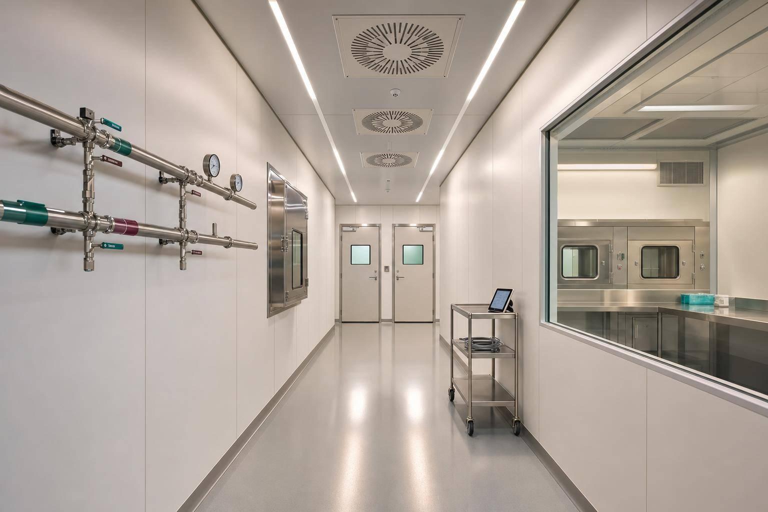
Cleanroom fit-out is often underestimated but is a critical factor in fab schedules. A staggering 87% of construction professionals cite delays as the biggest challenge in delivering semiconductor facilities [10]. Costs for cleanroom construction range from $10,000 to $20,000 per square foot, depending on the ISO classification [9]. Even when a facility looks complete, it may still be months away from being production-ready due to the demanding certification process.
Labor shortages make this phase even tougher. Skilled workers like welders, pipefitters, and electricians trained for ultra-clean environments are in high demand. A single semiconductor megaproject can require 500 to 800 welders on-site at its peak, which can overwhelm local labor markets [12]. These challenges not only delay production but also drive up costs significantly.
Schedule delays are a major factor in cost overruns, but they’re far from the only source. Costs can start to climb even before construction begins, often from multiple directions at once. To keep expenses in check, it’s crucial to understand the main drivers of these overruns, including equipment complexity, material prices, and labor challenges.
Semiconductor fabs are anything but typical industrial facilities. A state-of-the-art fab, which can cost $10–$12 billion, relies on highly specialized tools. One example is the ASML EUV lithography machine, priced at $350 million, which requires intricate logistics and precise installation [4][14]. In fact, installing tools like these accounts for about half of a fab’s total cost [4].
The complexity doesn’t stop there. Producing modern chips involves 80+ masks and thousands of process steps [2]. This means systems like process piping, ultra-pure water, chemical distribution, and HVAC must work seamlessly together. As Kaushik Krishnan, a Licensed Professional Engineer, explains:
"The biggest integration risks lie at the intersection of mechanical systems and high‐purity chemical distribution... Something that passes code in a conventional industrial facility will completely fail in an ultra‐clean environment." [1]
When these systems aren’t coordinated from the start, the fixes during commissioning can be far more expensive than addressing the issues during the design phase. Early integration is essential to avoid these costly pitfalls.
Building a fab in the U.S. comes with a hefty price tag compared to similar projects in Asia. For instance, constructing a U.S.-based fab costs $22–$28 billion, while a comparable facility in Taiwan ranges from $17–$20 billion - a 25–40% difference [15]. This pricing disparity extends to wafers as well. A 3nm wafer in the U.S. is expected to cost $22,000–$26,000, compared to $17,000–$22,000 in Taiwan. By 2026, 2nm wafers may reach $30,000 each [15].
This "onshoring premium" is a reality for any company building domestic capacity. Procurement teams that don’t account for this early on risk outdated cost models before construction even begins. One way to manage this is by securing long-term agreements with suppliers as early as possible to guard against further price hikes. Rising costs only worsen when unexpected design changes occur.
Fabs are typically built on fast-track schedules where design and construction overlap. This creates a high-risk environment where even small changes can have a domino effect. For example, a minor adjustment during the Front-End Engineering Design (FEED) phase can lead to rework across interconnected systems. When these changes aren’t properly documented, field teams may rely on outdated plans, resulting in failed inspections and expensive rework.
Rushed design reviews also amplify risks, as they can overlook utility constraints, safety gaps, or long-lead dependencies - issues that can derail startup timelines. Evann Smith, Digital Solutions Manager at Bechtel, describes it well:
"It is like flying a plane while you're building it... We're talking about dynamic and fluid projects that present both a challenge and an incredible opportunity." [4]
To combat scope creep, owners can assign dedicated gatekeepers to reject non-essential changes and use live, timestamped change logs instead of static spreadsheets. This approach helps keep budgets in check and minimizes disruptions.
Semiconductor fabs have utility requirements far beyond those of standard industrial facilities. They need stable, uninterrupted power and ultra-pure water. Even minor fluctuations in these systems can reduce yields by 0.5%, which translates to tens of millions of dollars in lost value annually [3]. As Kaushik Krishnan emphasizes:
"In semiconductor manufacturing, even brief instability can have significant operational consequences, so reliability matters just as much as capacity." [1]
Delaying utility planning can lead to costly retrofits, emergency procurement, and synchronization issues, all of which inflate costs and delay production timelines.
When schedules slip, a common reaction is to accelerate work by adding shifts, compressing timelines, and pushing crews harder. Unfortunately, this often backfires. Overextended crews see productivity drop, coordination falters, and mistakes increase. A case in point is TSMC’s Fab 21 in Phoenix, Arizona, which took about five years to reach production - much longer than similar projects in Taiwan. Labor shortages, unfamiliar local regulations, and adapting to local design rules all contributed to the delays [13][2].
A TSMC executive noted:
"After a painful learning curve, we have finally connected most of the dots and know which local construction contractors we can work with in building new plants." [13]
The takeaway? Vetting and establishing relationships with local contractors early in the process is one of the smartest ways to avoid costly delays later on.
Pinpointing cost and schedule drivers is only part of the challenge in managing a construction project. The other part? Setting up the right controls early enough to prevent small issues from snowballing into major problems. Owners who prioritize these measures from the outset - rather than reacting to problems later - tend to achieve better results in terms of both timelines and budgets. For a more detailed exploration of how these strategies apply to complex construction projects, check out the iRecruit construction project delivery guide.
One of the most impactful steps an owner can take is starting procurement as early as possible. For instance, advanced semiconductor equipment often needs to be reserved 18 to 24 months ahead of installation [12]. Waiting until designs are finalized before placing orders can almost guarantee delays.
"Many materials required to build a semiconductor fab have lead times of over a year right now." - Neil Nunez, Site Manager, Bechtel [11]
But timing isn’t the only factor. Building strong relationships with vendors provides early insights into potential lead time risks. Shozo Saito, President of the Nippon Electronic Device Industry Association, emphasizes the importance of partnership:
"Companies must move beyond the concepts of supplier and purchaser and approach suppliers as business partners." [16]
A practical example of this approach comes from Toyota Motor Corporation and Denso. By sharing supply chain data during the R&D phase and opting for standardized semiconductor components, they strengthened their buying power and minimized the risk of shortages [16]. Engaging vendors during the design phase - not just during procurement - allows owners to address risks proactively, laying the groundwork for smoother project execution across all components.
A semiconductor fab isn’t just a collection of independent work packages; it’s a highly interconnected system. The points where different packages intersect - like where mechanical, electrical, and plumbing (MEP) systems connect to process piping or where structural work meets cleanroom fit-out - are often where the most costly surprises occur. To address this, owners need a governance structure that prioritizes these interfaces as key risks.
This involves setting up regular review cycles with clear decision-making accountability at every stage and using shared data platforms so all stakeholders - engineering, procurement, and construction teams - have access to the same live information. Evann Smith, Digital Solutions Manager at Bechtel, highlights the value of this integrated approach:
"Because the opportunity for influence is highest early, from a data perspective we need to be integrated from the beginning with transparency amongst partners." [4]
When off-site manufacturing (OSM) is part of the project - an increasingly common strategy to reduce on-site labor congestion - logistics and rigging experts must be involved from the design phase, not brought in as an afterthought [4].
Even with early vendor engagement and solid governance, managing changes effectively is critical. On fast-track projects like semiconductor fabs, scope changes are inevitable. The key isn’t to avoid them entirely but to address them early, when they are less costly. Ricky To, Senior Manager of Data & Digital Delivery at Exyte, explains the shift in mindset:
"By changing the approach from failing slow to failing fast, fab builders can shift the bulk of the risk of changes from late to early stages while reducing material waste and cost of delays." [4]
This proactive approach helps protect both the schedule and the budget. It requires enforcing design review rigor, even when tight timelines might tempt teams to skip steps. For example, Kaushik Krishnan’s team applied strict engineering controls to mechanical and process safety decisions across a multi-billion-dollar manufacturing portfolio. Their disciplined approach shaved 4 months off the schedule and avoided approximately $200 million in potential rework and downtime costs [1]. The takeaway? Cutting corners on design reviews to save a couple of weeks can lead to far bigger delays and costs down the line.
Traditional project management tools often fall short on complex builds where a single delayed decision can disrupt numerous interconnected work packages. Owners need systems that provide real-time risk visibility. A data mesh architecture, which synchronizes engineering, procurement, and construction tools, ensures all partners work from a single, up-to-date source of information, eliminating delays caused by siloed communication [4].
Digital twins offer another layer of control. Samsung, for example, has been testing digital twin platforms to simulate physical spaces and cyber-physical systems before construction begins [4]. By integrating data across engineering, procurement, and construction in real time, these tools help owners anticipate design changes and make faster, more informed decisions throughout the project lifecycle.
Semiconductor Fab Construction: Phases, Timelines & Key Milestones
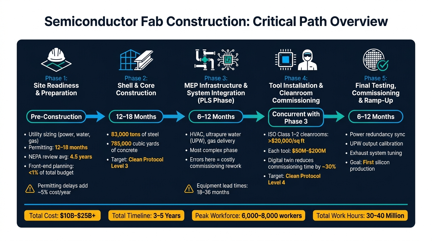
Building a semiconductor fab is like orchestrating a complex symphony - each phase must be perfectly timed, as delays in one part can disrupt the entire project. To keep things on track, experienced project managers often rely on reverse scheduling. This method starts with the end goal - tool qualification - and works backward to establish milestones along the way [9]. It’s a strategy that prioritizes realistic timelines over overly optimistic ones, ensuring every phase builds seamlessly on the last.
The first step in any fab project is preparing the site, which requires careful coordination. Kaushik Krishnan, Global Manufacturing Leader, highlights the importance of an integrated approach:
"Semiconductor expansion will move fastest where site selection, utility planning, and industrial infrastructure investment are treated as one integrated strategy rather than separate workstreams." [17]
Utility sizing - covering essentials like power, water, and specialty gas - needs to be addressed early in the front-end engineering phase. While this step accounts for less than 1% of the project’s total budget [12], skipping it can lead to costly delays during production ramp-up. Permitting and regulatory hurdles often stretch timelines, making early planning even more critical. For those interested in the broader challenges of infrastructure planning, the iRecruit power and energy infrastructure guide offers helpful insights.
Constructing the facility’s core and shell typically takes 12 to 18 months and includes the installation of main utility systems [9]. By the end of this phase, the facility should reach "Clean Protocol Level 3", meaning it’s in a positive pressure "blow down" state and ready for the next steps. Building a fab of this scale is no small feat - it usually requires around 83,000 tons of steel and 785,000 cubic yards of concrete [9]. This structural foundation is essential, as everything from cleanroom floors to high-tech equipment installations depends on its stability.
With the shell complete, the focus shifts to the Process Lateral Systems (PLS) phase, lasting 6 to 12 months [9]. This stage involves integrating mechanical, electrical, and plumbing systems with critical networks like HVAC, ultrapure water lines, and gas delivery systems. Precision is key here - any errors can lead to defects during commissioning, which are not only costly but also time-consuming to fix [1]. Once these systems are in place, the next priority is creating a carefully controlled environment to support tool installation.
When the cleanroom achieves "Clean Protocol Level 4", crews begin installing tools on vibration-dampened platforms. Each tool, costing anywhere between $50 million and $200 million, requires precise commissioning [9]. Constructing ISO Class 1–2 cleanrooms, particularly for advanced EUV lithography, can cost over $20,000 per square foot [9]. To streamline this process, many builders now use AI-powered digital twins. These virtual models allow teams to test tool hookups and airflow configurations before physical installation begins. As Herbert Blaschitz, Executive VP at Exyte ATF, explains:
"With the digital twin, we can basically commission the fab without the fab being built. This helps to spot obstacles and even reduce operating costs." [9]
This approach can shave about 30% off physical commissioning time [9].
The final phase, lasting 6 to 12 months, involves synchronizing systems like power redundancy, ultrapure water output, and exhaust systems to prepare for production [9]. Even with the site fully built, fine-tuning is often necessary before wafer production can begin [1]. These last steps highlight just how much coordination and precision are required throughout the entire process to deliver a fab that’s on time and within budget.
Building a semiconductor fab is no small feat - it demands an incredible 30–40 million work hours and can peak at a workforce of 6,000 people [9]. Without the right leadership in place from the very beginning, even the most detailed plans can fall apart. This can lead to unnecessary delays and skyrocketing costs. To keep things on track, owners need to prioritize hiring key roles early to mitigate risks effectively.
Some of the essential early hires include project executives, cost estimators, schedulers, and specialized MEP (Mechanical, Electrical, and Plumbing) leaders.
For those navigating the complexities of large-scale fab projects, the iRecruit construction project delivery guide provides valuable insights into how early hiring decisions can shape the success of mission-critical builds.
Project executives should be brought on board during the early planning stages, where they can tackle critical tasks like regulatory oversight. They play a pivotal role in implementing the backward pass approach across the project's multi-phase structure - Base Build, Process Lateral Systems, and Tool Install.
"Successful ramp-ups depend on teams that can coordinate engineering design, supply chain readiness, facility infrastructure, and operational execution simultaneously." - Kaushik Krishnan, Global Manufacturing Leader [1]
In the U.S., fabs take about twice as long to build as their counterparts in Taiwan, largely due to permitting challenges [9]. This highlights the importance of experienced leadership to navigate these hurdles early on.
Cost estimators handle some of the most significant financial aspects of fab construction, from managing $50 million to $200 million process tools to overseeing cleanroom construction, which can exceed $20,000 per square foot for ISO Class 1–2 environments [9]. Their expertise ensures that budgets are realistic and well-managed.
Schedulers, on the other hand, bring advanced tools like AI-driven planning and digital twins into the mix. These technologies can cut delays by up to 30% during virtual commissioning [9]. By incorporating these tools into the project’s master schedule, owners gain a competitive edge in speeding up timelines without sacrificing quality.
The Process Lateral Systems phase (Phase 2) is often considered the most challenging stage of fab construction [9]. This phase involves the integration of ultrapure water lines, specialty gas delivery networks, and high-capacity HVAC systems. As Masroor Malik, Lead Solutions Specialist at Swagelok, explains:
"Fluid management systems... function essentially as the semiconductor fab's circulatory system by transporting liquids and gases where needed throughout the facility." [3]
MEP leaders with expertise in this highly specialized environment are crucial. A single misstep, such as a misaligned utility connection or contamination, can cause months of delays and cost tens of millions of dollars [9]. Commissioning leaders also play a vital role, ensuring that all systems are properly integrated and functional before they go live. Waiting to hire these specialists until after MEP installation is a costly error that owners should avoid.
Building a semiconductor fab is one of the most complex and demanding projects in modern industry. A state-of-the-art facility can cost a staggering $10 billion to $12 billion, require a workforce of 6,000 to 8,000 people, and take two to three years to complete from groundbreaking to first silicon [4]. With such tight margins for error, even minor missteps can lead to significant setbacks.
The key to success lies in integrated planning from the very beginning. Treating the fab as one cohesive engineering system, rather than a collection of separate contracts, ensures that critical elements like design, procurement, utilities, and workforce strategy are aligned from day one. As Kaushik Krishnan, Global Manufacturing Leader, explains:
"Speed becomes sustainable only when engineering discipline, compliance, and reliability are built into the deployment model from the beginning." [1]
Adopting off-site manufacturing (OSM) for at least half of labor hours and embracing a fail-fast design approach has proven to deliver better results compared to traditional linear construction methods [4]. Additionally, investing in thorough front-end planning - typically costing less than 1% of the total project budget - provides the highest return on investment [12].
Another critical factor is addressing workforce challenges. The U.S. semiconductor industry is expected to face a shortage of 70,000 to 90,000 workers in the coming years [18]. To mitigate this, hiring key personnel such as project executives, cost estimators, schedulers, and MEP commissioning leaders early in the process is essential. Strategic early hiring not only reduces risks but also sets the foundation for a smooth project execution. For owners seeking guidance, iRecruit.co's construction project delivery guide offers practical advice on structuring teams for high-stakes builds.
The formula for delivering a fab on time and within budget is straightforward: align all aspects - design, procurement, and workforce - under a unified strategy. Early planning, securing critical components, managing scope, and assembling the right team are the building blocks of success. Every decision made at the start has a lasting impact on the project's ultimate outcome.
The journey to achieving first silicon involves navigating through several crucial stages: design, tapeout, manufacturing, and validation.
Any delay - whether caused by design flaws, production bottlenecks, or supply chain disruptions - can significantly push back the timeline, making each phase critical to success.
Owners need to secure long-lead tools and utilities during the planning and early construction phases - ideally 3 to 5 years before production starts. Doing so helps ensure these critical components are delivered on time, reducing the risk of expensive delays. Early commitments like this are key to staying on schedule and navigating the complex challenges of building semiconductor fabs.
Early and detailed planning is key to steering clear of costly late-stage scope changes. Leveraging AI-driven tools and virtual simulations can help spot potential issues before construction kicks off, minimizing surprises. For intricate projects, such as semiconductor fabs, collaborating early with specialized engineers and suppliers is essential. This approach tackles potential changes upfront, keeping budgets and timelines on track. A well-defined project scope from the start is crucial to sidestep expensive revisions down the road.